Monday, May 16, 2016

Gradiente MS M320 – Mini Component System Circuit Diagram

Used ICs: TB2132FN – TC4052BP – BA3308 – LA4627 – SC9153A
Schematic [Click on the schematics to zoom in]

Thursday, May 12, 2016

Philips Saturn 563 – Vacuum Tube Radio Schematic

Used Valves (Tubes): ECH81 - EF89 - EBF89 - EABC80 - EM80 - EL86 - EZ81
Schematic

Wednesday, May 11, 2016

Staner uPA8000 Amplifier 1600Watts RMS – Circuit Diagram (Schematic)

1600W per Channel - Staner uPA 8000 Hi-Power Amplifier - Circuit Diagram
Circuit diagram

Tuesday, May 3, 2016

Akira HTS 38DVD Schematic

AKIRA Home Theatre System – Circuit Diagram
Schematic - Tuner [Click on the schematics to magnify]
SMPS
Center and sub
Front Left & Right

Monday, May 2, 2016

RCA – THOMSUN ICC1 Chassis – CRT TV – Circuit Diagram

Used ICs: TDA2542 – MC14053 – TDA1048 – TDA1180 – TDA3030A – TDA1170S – TDA3300
Schematic
Click on the schematic to zoom in

Saturday, April 30, 2016

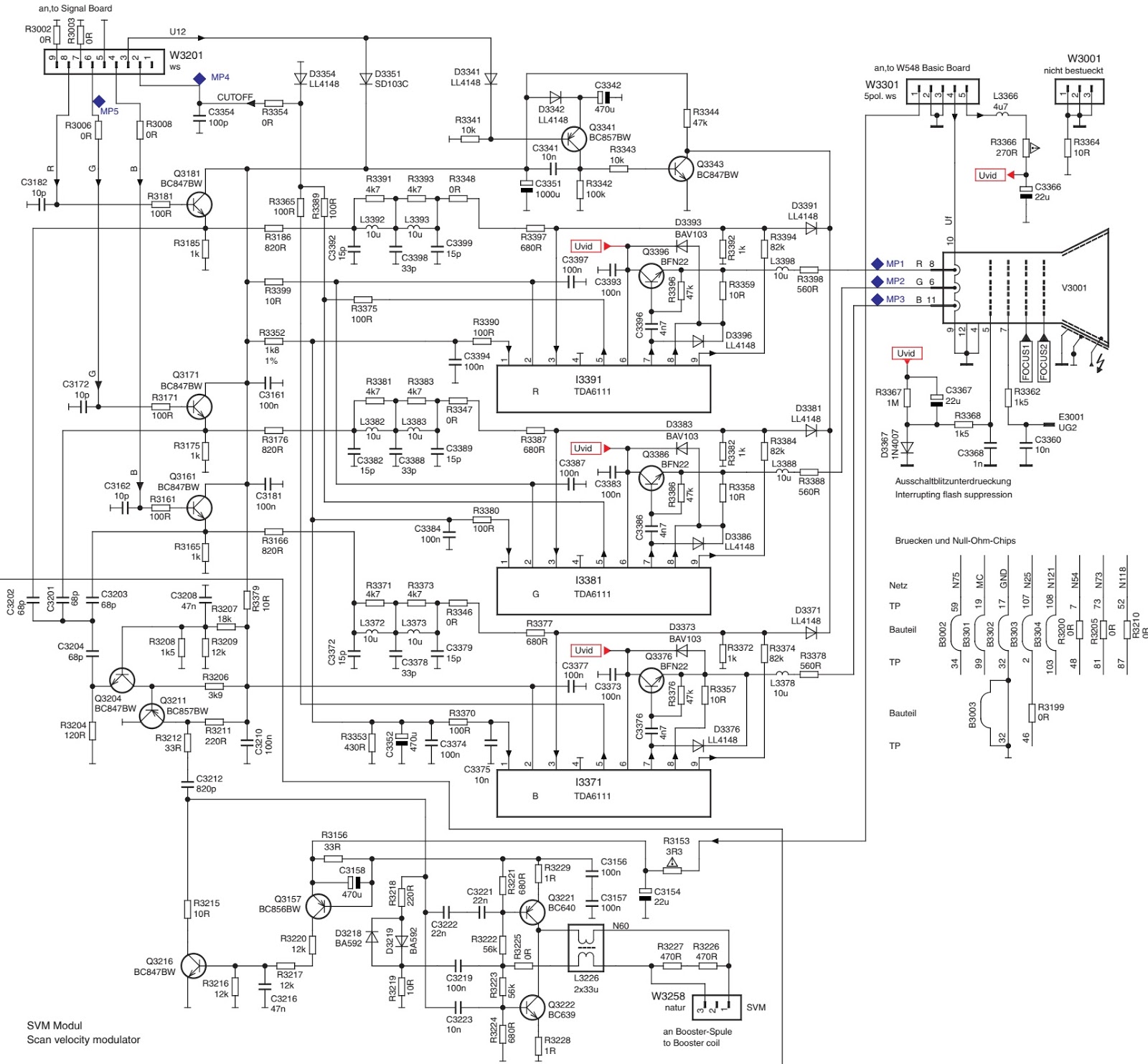
Loewe CRT TV - Circuit Diagram

Used ICs: TDA7296 – TDA4653 – BUZ91A(FET) – TEA6422D – TEA6415 – MSP3411 – MC33079 – VPC323 – M27V322-100 EPROM – TS831-3IDT – SDA9488 – TDA9332-N2 – TSA5523M – TDA6111 – LM2574 – TE28F008 – KM416V – STI5500 – STV299B – CS4344 – LM2574M – MAX4546 – STV0056 – TDA6151-5X  
Schematic
Click on the schematics to zoom in

Thursday, April 21, 2016

LG RZ32LZ55 - 32 inch LCD TV - Schematic

Video control and display data:  Video signal is received from TUNER, AV port(AV1,AV2,S-Video,Component) and goes to the one-chip video decoder (VCTI) which separate the R,G,B signal and passes on the signal to AD converter(AD9883) which converts 4:4:4 video format into digital and gives output to the Picture Enhancer(FLI2300).This picture enhancer improves the quality of the picture by changing the level of RGB signals. The output of this enhancer chip is fed to the deinterlacer ,which in turn goes to the Scalar (GM5221).The scalar gives the output on the LVDS cable which is connected to LCD module.  VCTi acts a micom and is responsible for video processing and audio signal processing. It accepts the RF signal and separates sound and picture from it.  Scaler is responsible for regulating the timing of signal to LCD panel and size and location of the signal. Graphic control accepts the PC(Analog RGB) and DVI-D (Digital ) signal, Scalar is responsible for regulating the timing of signal to LCD panel and size and location of the signal. Graphic control accepts the PC(Analog RGB) and DVI-D (Digital ) signal,the signal of PC input is connected to analog port in Scaler and the signal of DVI-D input is connected to digital port. Thus it receives two input and switch between them to give output at the LVDS which in turn gives output at the LCD module.
Schematic
Power unit: The power board supplies a DC voltage of 33V, 24V, 12V to the main board.out of this 33v is used by the tuner and 24v is used directly by the inverter and the sound amplifier IC. 24v also is converted into 5v by a regulator.  The 5v is changed into 3.3v and 1.8v by a regulator, both voltages(3.3v, 1.8v ) is used by VCTI, Scaler, FLI2300 and AD9883. The voltage of LCD Panel is 12v.

RZ26LZ55 LG LCD TV - Circuit Diagram

Power unit: The power board supplies a DC voltage of 33V, 24V, 12V to the main board.out of this 33v is used by the tuner and 24v is used directly by the inverter and the sound amplifier IC. 24v also is converted into 5v by a regulator.  The 5v is changed into 3.3v and 1.8v by a regulator, both voltages(3.3v, 1.8v ) is used by VCTI, Scaler, FLI2300 and AD9883. The voltage of LCD Panel is 12v.
Schematic
Video control and display data:  Video signal is received from TUNER, AV port(AV1,AV2,S-Video,Component) and goes to the one-chip video decoder (VCTI) which separate the R,G,B signal and passes on the signal to AD converter(AD9883) which converts 4:4:4 video format into digital and gives output to the Picture Enhancer(FLI2300).This picture enhancer improves the quality of the picture by changing the level of RGB signals. The output of this enhancer chip is fed to the deinterlacer ,which in turn goes to the Scalar (GM5221).The scalar gives the output on the LVDS cable which is connected to LCD module.  VCTi acts a micom and is responsible for video processing and audio signal processing. It accepts the RF signal and separates sound and picture from it.  Scaler is responsible for regulating the timing of signal to LCD panel and size and location of the signal. Graphic control accepts the PC(Analog RGB) and DVI-D (Digital ) signal, Scalar is responsible for regulating the timing of signal to LCD panel and size and location of the signal. Graphic control accepts the PC(Analog RGB) and DVI-D (Digital ) signal,the signal of PC input is connected to analog port in Scaler and the signal of DVI-D input is connected to digital port. Thus it receives two input and switch between them to give output at the LVDS which in turn gives output at the LCD module.